ATE Services
Through Pactron's ATE board development solutions, semiconductor manufacturers gain access to expertise and resources essential for designing, developing, and manufacturing top-tier ATE boards. These boards adhere to the rigorous standards of semiconductor testing, ensuring high quality and reliability.
These solutions contribute to reliable, accurate and efficient testing processes, leading to improved quality control, increased productivity and reduced time-to-market for semiconductor devices. Pactron Specializes in ATE hardware, facilitating accurate testing and measurement of the Device under tests performance & functionality.
- Universal probe cards
- Device interface board
- Handler interface boards
- Load boards
- Probe interface boards
- Characterization boards

Final Test Board
Pactron provides customized solutions designed to meet specific IC testing requirements, ensuring accurate and reliable interfacing between the device under test and automated test equipment.
- Experience in all major ATE platforms – Teradyne, Advantest, Nextest, Chroma, NI & other platforms.
- Simulation Correlation - TDR Measurement on board to verify back drill stub effect.
- Decoupling Scheme Recommendation to meet transient current requirement.
- Power Integrity – IR Drop Optimization, Site to Site correlation.
- Step Drilling for Test Pogo vias, via modelling for high frequency, optimized pogo footprint.
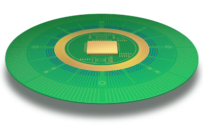
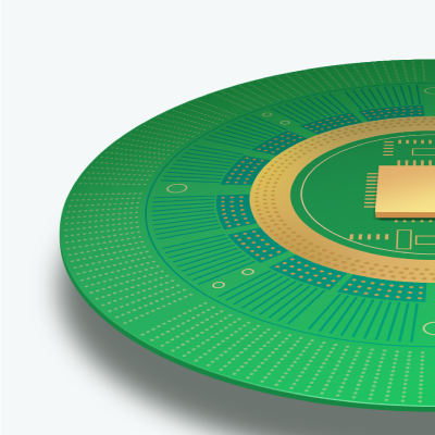
Probe Cards
Pactron offers advanced technology and design services to create precise and durable cards suitable for wafer-level testing, ensuring high-quality and efficient testing for semiconductor wafers before they are packaged.
- Blind Vias for > 20GHz to eliminate stub effect
- Impedance optimization for BGA Vias, BGA Breakout region, Differential Via Modelling, Die pad optimizations.
- Hybrid PCB Stack up with Low Dk Material for High-Speed layers Megtron7, Megtron6, Rogers 4003C, Rogers 4350B etc.,
- Max Layer Count – 82 Layers/ PCB Size/Diameter – Up to 520 mm
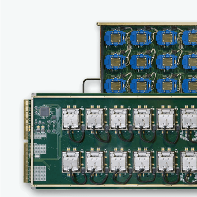
Reliability and Burn-in-Engineering
Pactron is a leading provider of specialized design and manufacturing services for a wide range of Reliability PCBs specifically tailored to meet the stringent requirements of semiconductor companies.
- HTOL
- HAST/THB
- HBM/LU Boards
- MCC – LC2
- AEHR MAX 3
- REL INC
- Delta – V (PTC)
- Program Cards/Coupon Boards/ADAPTER Boards
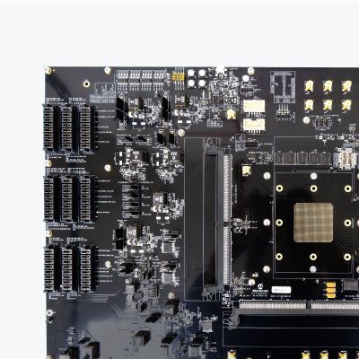
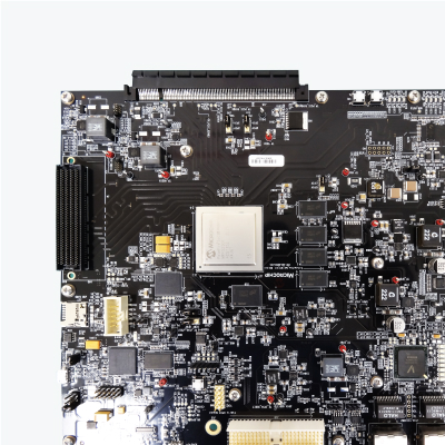
IC Characterization Board
At Pactron, we recognize the pivotal role that characterization boards play throughout the device development, testing and validation phases. Our hardware development platform for characterization facilitates crucial evaluations, including performance assessment, vital parameter measurement, calibration and IC validation. Leveraging our expertise in hardware design, signal and power integrity simulations, intricate PCB layout and high-quality PCBA, we serve as the ideal design partner for achieving successful IC development.
- Requirement Analysis
- Hardware Design and Prototyping
- Signal Integrity and Performance Optimization
- Software Development and Integration
- Testing and Validation
- Documentation and Support
Reference Design & Development
Pactron provides tailored IC Reference Kit development services designed to meet specific requirements. Through our expertise in customized IC Reference Kit development, semiconductor developers can accelerate the design process, validate performance and guarantee the quality of their integrated circuits. This results in faster time-to-market and increased competitiveness within the industry.
- Requirement Analysis
- Hardware Design and Prototyping
- Signal Integrity and Performance Optimization
- Software Development and Integration
- Testing and Validation
- Documentation and Support
Turnkey Build & Kit Development
Pactron's PCB turnkey build services, inclusive of kit development, deliver seamless solutions from initial concept to final delivery. We employ state-of-the-art PCB fabrication, precise assembly techniques, efficient inventory management, meticulous kitting, comprehensive test coverage and timely shipment. This ensures optimal execution of New Product Introduction projects (NPI) and small volume proto builds.
Key elements encompass:

PCB Assembly:
Precise fabrication and assembly of printed circuit boards according to specified requirements.

Inventory Management:
Efficient tracking and management of electronic components, guaranteeing their availability throughout production.

Kitting:
Methodical compilation of all essential components into organized kits, enhancing the efficiency of the assembly process.

Shipment:
Coordination of logistics to ensure timely delivery of kits to end-users or production facilities, optimizing project timelines.

Kit Documentation:
Thorough documentation accompanying each kit, providing comprehensive guidance and reference for assembly and usage.